Introduction
ITDev recently engaged with an ASIC design company who were looking for some digital engineers to support their development team. They were creating a test chip as a precursor to their main silicon design project, with the idea that some key features could be tested on-chip prior to the final design going out for fabrication. Given the tight deadline it was important to ensure that our design process was as efficient as possible, but at the same time, ensuring that the design worked correctly meant that we did not want to compromise on verification. This blog outlines our verification strategy, and how our knowledge of UVM allowed us to achieve high test coverage in a very short time.
Block level testing vs System level testing
Block level simulation is an important part of agile digital development, since ironing out any bugs at the module level can make system level verification go much more smoothly. As the design matures, testing at the block level usually takes a back seat, and testing at a higher level becomes more important. This gives rise to some questions: how much time is it worth investing into a block level testbench if we know from the outset that as the design progresses it will lose some of its value? Might it not be more efficient to wait until the design is mostly complete and perform testing at a high level instead? The answer to both questions is, of course, that it is up to the designer. Finding a good balance between effective block level testing and the need to progress a project is something that depends on the experience of the engineers and the time they have available. Luckily for us, UVM has several features which made finding that balance a little easier.
The UVM framework
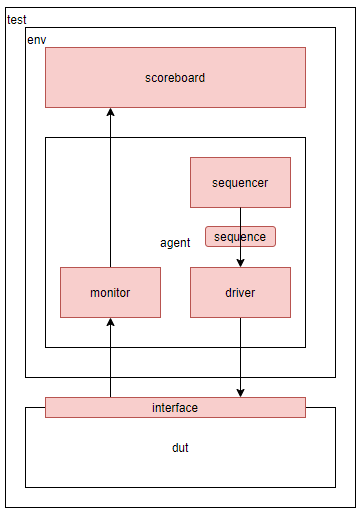
Figure 1: simplified UVM testbench framework
For those unfamiliar with the framework of a UVM testbench I will give a simplified explanation alongside the block diagram shown above.
- A test sequence contains information about the stimulus desired on the DUT interface. Multiple sequences can be run during a test, the sequencer is responsible for sending them to the driver.
- The driver receives a sequence item and decodes it, then drives the DUT interface in the requested manner.
- The monitor captures information about what is happening on the DUT interface. It builds transactions containing this information about the interface behaviour, which are then sent to the scoreboard.
- The scoreboard checks these transactions and determines if the behaviour of the interface is valid.
A very detailed description of the UVM framework can be found here: https://verificationguide.com/uvm/uvm-testbench/
I stated in the introduction that we are aiming to find a balance between block level and system level testing, this is where the reusability of UVM components comes in to play. The components in Figure 1 which are highlighted in red are the ones most readily reused as the design grows. The ability to abstract these components and move them to a higher level testbench means that if thorough block level testing is implemented, testing at the top level simply becomes a process of moving around existing components. I will demonstrate with a simple example.
Example verification flow
We have a module named frame_check which we wish to validate at block level. It accepts data frames on its input interface, performs validation checks which discard any frames which do not meet its validation criteria, and passes along those which do.
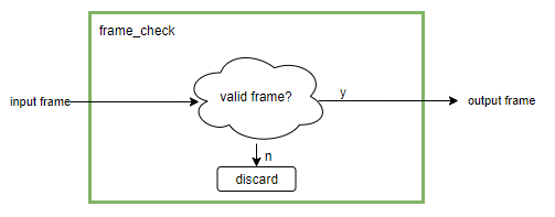
Figure 2: frame check module
We build a UVM testbench for frame_check as shown in Figure 3:
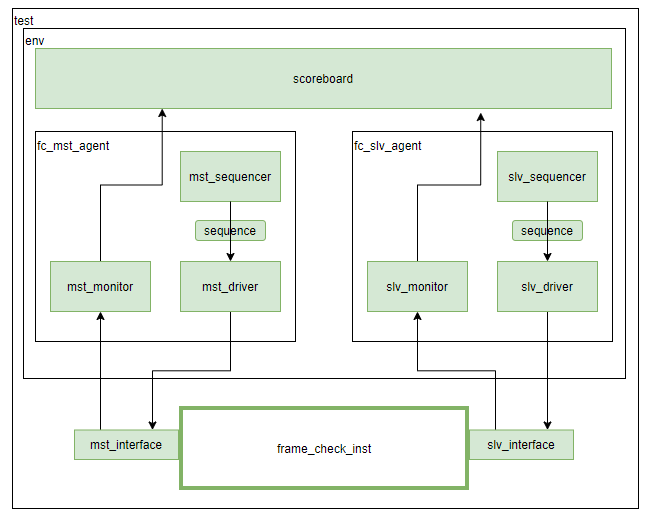
Figure 3: frame_check testbench
The test is straightforward. A sequence is created instructing the driver to push a mixture of valid and invalid frames onto the input interface of the frame_check module. The monitor captures this and sends a transaction to the scoreboard each time a valid frame is driven to the DUT. The monitor captures input and output ports of frame_check, gathering the input and output frames to send to the scoreboard. The scoreboard now has the following information: which frames were driven to the DUT and in what order, and which frames were seen on the output and in what order. The scoreboard verifies that only valid frames were passed through, and that no invalid frames were seen on the output port of frame_check. The test passes and we are now sure that frame_check is working as expected, so we move on with the next stage of the design.
A decoder is developed to convert a serial interface into our data frames.
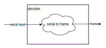
Figure 4: decoder module
A block level testbench has also been developed for the decoder block, complete with a driver, monitor and scoreboard of its own. The integration phase begins and several modules are instanced to create a higher level module called frame_capture_block, shown in Figure 5.
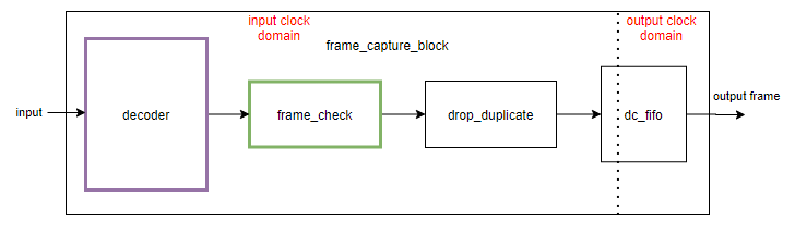
Figure 5: frame_capture_block
We now have four modules instanced together. The decoder decodes the input data and builds the received frames. The frame_check module checks the frames are valid, the drop_duplicate module discards repeated frames, and there is a dual clock FIFO for passing output frames onto an output clock domain.
At first glance it may seem that the testbench created for the frame_check and decoder modules are now of little use, and that we will need to start again in developing a testbench for this group of modules. However, if we think a little harder, it becomes clear that most, if not all, of our existing verification code can be reused with little effort:
- Sequences
The test sequence developed for the decoder testbench can be reused – all that we require is that a mixture of valid and invalid frames are driven into the design. - Monitors
The monitor for the frame_check testbench will monitor the output of the frame_capture_block (albeit on different clock than before).
The monitor from the decoder testbench will capture information entering the decoder block. - Scoreboards
The scoreboards can be combined, with a slight addition to the frame_check scoreboard to allow duplicate frames to be dropped. - Drivers
The driver developed for the decoder testbench will be reused to drive data into the module.
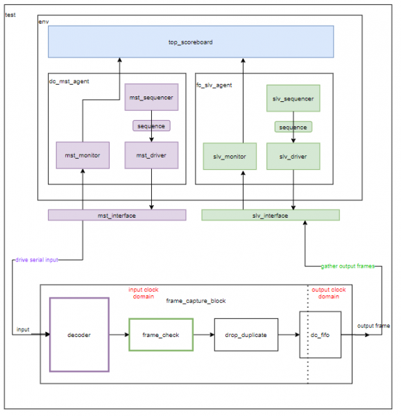
Figure 6: high level testbench built using components from lower level testbenches
This simple example shows how a higher level testbench has been created entirely using components pulled from the block level testbenches of its component modules. As the design grows further the expectation is that many of these components will be reused again in higher level testbenches.
Conclusion
For the purpose of demonstration, the example given was a very ‘friendly’ one, in that it was easy to reuse the testbench components. In reality it is often necessary to carefully plan not only where block level testing will be most useful, but also where the testbench components will have maximum reusability. As seen in the example, standardisation of interfaces throughout the design will also improve reusability of verification components. We can summarise this ‘design for reuse’ verification strategy with a single point; block level testbenches should be an opportunity to create design components which will eventually be used for system level testing. Keeping this idea in mind when deciding which blocks to test individually allows for targeted verification at low level, while simultaneously developing tools to accelerate verification at system level.
Returning to the question posed in the introduction ‘might it not be more efficient to wait until the design is mostly complete and perform testing at a high level instead?’ We can now see how, if used properly, this verification strategy negates the need to consider such a situation.
How ITDev Can Help
At ITDev we believe good engineering practice is essential to delivering high quality, engineered designs. Aligned with this, we run a series of events and workshops to help develop industry best practices through collaborative sharing and learning.
ITDev provides technology consultancy as well as hardware & software design services; our team of engineers has extensive experience in RTL design for both FPGA and ASIC.
If you have any questions or would like to find out how we can help you, initial discussions are always free of charge and we would be delighted to speak to you. Email us or call us on +44 (0)23 8098 8890.